
Figure 1 - unpacked
The first step was to lay out the enclosure, cut some holes, and drill some bolt holes. The printed directions had a well dimensioned drawing, alas it was not to scale. No worries. I set forth laying out the front panel by using the board as a template, with an accurate metric scale to verify the measurements. A set of drafting dividers provided pinpoint accuracy when marking the cutouts and holes.

Figure 2 - Laying it out
The double-sided board is very high quality with a great ground plane.

Figure 3 - cutting the holes
The tricky parts were making the square holes in the plastic project box. This was done using a roto-zip bit in my Dremel tool. Marking out the limits with blue painters tape gave a good contrast when routing out the shapes. The holes had to be absolutely accurate to allow everything to line up.

Figure 4 - Cutouts

Figure 5 - Completed cutouts
The side adjustment for the tuning capacitor was the most difficult part. I used a "flapper wheel" emory tool for the Dremel to smooth the shape of the cutout.


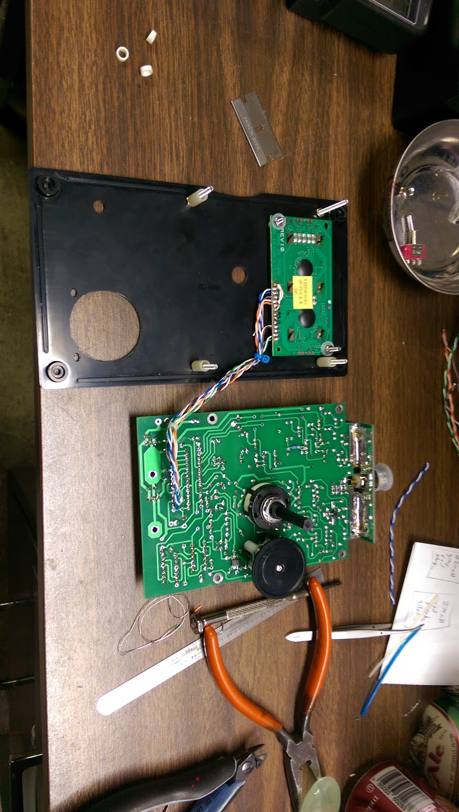
Figure 6 - Connector board to Main Board
The connector board is conveniently marked with centering tracks to aid in getting the boards to mate just right. Following the directions, tacking the boards together first is critical before applying a drafting square to to insure a 90 degree match between the surfaces. The first components to be added were the surface mount devices, which go on the trace side of the board. These SMT components are very small and just a little heat is needed to put them in place while holding them steady with a pair of forceps. It should be noted that reading the directions closely is imperative while positioning the surface mount transistor, since the label on the part goes DOWN towards the board.

Figure 7 - Resistors
Each resistor was carefully verified with my trusty DVM (Digital Volt Meter) before soldering it carefully in place. The leads could then be clipped off on the track side. The directions recommend doing the smaller components first and then following up with the larger and higher components. This makes very good sense so that the clearance of placing the smaller components is easier without the larger components in the way.

Figure 8 - Track side of the board with resistors
Adding the diodes and capacitors came next. I was confused at first because the kit came with two extra 100nF caps. I double checked the inventory count to make sure I wasn't missing something. There are only the ones called for required and indeed the kit had two extra.

Figure 9 - Capacitors
The kit instructions were careful to mention that the caps should be tight against the board with no lead length above the board surface. This reduces stray capacitance. There is a note to actually leave the 68pF cap above the board surface for a better result and along with R31, R32, diodes D2, and D3. I actually went back later and read the errata notes, and raised them up more. I'll mention that again further on in the build report.

Figure 10 - Sockets
Adding the sockets for the IC's was a bit tricky while holding them flush and tacking one pin on each side. Once they start going wampus its hard to correct it, so I made sure they were flush before soldering each pin in place.

Figure 11- Transistors
The FET's (Field Effect Transistors) that came with the kit were selected as matched sets, so the test circuit provided in the instructions was not needed. The BJT's (Bipolar Junction Transistors) were also tested with the transistor checker gain feature on my DVM. The kit noted that all are not created equal and the position of the pins should be verified on each device. This was easily done after pre-bending the transistor leads carefully with a set of sharp needle-nosed pliers. Adding the trimmer pots was also an easy task since they are all the same value, with the exception of the display contrast adjustment, which can't be mistaken since it has a different form factor. The 6 multi-turn pots should be installed per the included assembly diagram. This is important per the direction so that an increase in measured voltage on the Test Point terminal increases with Clockwise rotation and decreases with Counter Clockwise rotation.

Figure 12 - Inductors
The last tricky part was the inductors which were thankfully packaged separately in the kit! Since I'm colorblind it was hard enough telling the resistors apart. The inductors were also verified with my inductance adapter for my DVM. This little adapter is a great tool. I've had it for years and totally takes the guesswork out of inductors.

Figure 13 - Selector switch
Reading the directions for the selector switch was actually the least clear point of the directions. I had to read it over and over to make sure I was doing it right. To aid posterity, the ALPHA selector switch is marked with pins 1 - 12 around the edges. Set the stop pin per the instructions at pin 6. This is done by removing the nut from the shaft, and re-positioning the stop into the number 6 hole. Looking at the selector Pin 12 goes to the 12 o'clock position with the antenna connector at the top. I verified it all twice with the continuity checker before soldering in place. The little wire inductor is a stretch across the center common pins. I bent the switch pins and carefully fit the inductor and the small connector lead at the 10:30 position using a piece of clipped component lead. Once again make sure everything is flush against the board before tacking the switch into place.

Figure 14 - Switch in place

Figure 15 - Tuning Capacitor
The tuning capacitor threw me for a loop at first. The leads were coming out the wrong side. You must remove the plastic cover from the back and put the leads out the bottom away from the shaft, before putting the plastic cover back on. They are VERY thin, so be careful that they don't break when turning them 180 degrees.

Figure 16 - Mounting the Display
I don't trust double-sided tape, so I made four additional holes to mount the display. The directions assume that you know which way is UP on the display. The terminals 1 to 14 go down towards the selector switch. I used 3mm bolts and spacers to set the display permanently in the front panel. The last think you want is for double-sided tape to fail and short the display into the main board!

Figures 17, 18 - Display Mounted permanently
To my annoyance the wire that was intended for the display did not accept solder readily. I tossed it aside and used some nice CAT-5 wire for the 9 connections from the display to the main board. A few pins are common on the main board, which conveniently allowed for less wires to be run. The pins 7,8,9,10 on the display were shorted with a bare wire and a jumper from 1 to 5 installed.

Figure 19 - Mounting Check
The board was then test-mounted to the front panel to check the spacing. 21mm listed in the instructions wasn't quite the right reference point. I determined the actual distance based upon the thumb wheel clearance to the front panel. The measurement was actually 21mm from the nut securing the bolt to the front panel with reference to the board's track surface.

Figure 20 - Test Fit
Patience and careful measuring paid off. Everything lined up. I used the soldering iron to melt the locating ring of the power switch into the front panel. It was more easier than drilling a hole. The selector switch shaft had to be cut off with a Dremel plastic cutting disk as it was far too long.

Figure 21 - Watch for smoke
While this photo doesn't capture it, the directions say to only insert IC1 and test it first. The output was verified with the 'scope to insure that a nice sine wave was being generated at the correct specifications. Setting the corresponding pot was also done. The other chips are added per the instructions setting each corresponding pot. Here's where the first problem arose. I could not obtain a 5v full scale on pot P3. I fiddled with the components associated with that circuit and discovered that if they were raised more from the board's ground plane an appropriate reading could be obtained.

Figure 22 - Success
While I didn't have exactly the right adapters to get a 50 ohm dummy load onto the antenna connector some quick scrounging in the parts bin yielded a workable solution. A few more tweaks on the calibration procedure got a perfect 50 ohm digital (and analog meter) reading with 1.0:1 SWR and 0.0 reactance. I was breathing a little better at this point. This simple verification made me feel that the build was successful. The front label could be safely applied. The label had to be cut out to accommodate the display, which was done with a straight-edge and a razor blade. The selector and power-switch holes were clearly marked. I punched them through with a set of leather punches and used them to locate the label roughly. The final precision location was done by the display cutout before pressing the label down permanently.

Figure 23 - Finished Product
This is a sharp-looking instrument. The last build aspect is to add the battery pack. Once again I don't trust double-sided tape. The battery holder has mounting holes, and really should be bolted in. Non-Skid feet on the back side of the instrument is probably needed to keep the instrument sitting level on the table.
The final test would be to compare the performance of the VK5JST analyzer against a commercial unit to verify the accuracy. There are issues with the build however, and I haven't been able to resolve them presently.
Remember the adjustment of P3 that I could not obtain full scale? I cannot obtain much more than half scale with the pot fully clockwise. I went back again and this time removed the components from the ground plane side of the board. After verifying them, I re-installed them on the trace side of the board. There was no significant change here, so the problem must be elsewhere. More study and research is needed on this subject. This is what is happening. I got a good N-Connector to BNC adapter so I could put a good terminating resistor on the instrument. With some reasonable tuning on P3, P4, P5 and P6 the instrument DOES indicate a reasonably reliable reading of about 50 ohms across all the band settings (with no reactance). A little fiddling with the P3 adjustment while the 50 ohms was installed, I could obtain a 50 ohm reading on the analog meter. Feeling rather pleased with myself, I then swapped the 50 ohm BNC terminating resistor with a 75 ohm BNC terminating resistor. The instrument reads approximately 30 ohms. I'm defeated at this point on this subject and have to admit failure.
The second issue was discovered while tuning around in the 10meter band. The display cuts out to zero and does not indicate any frequency above approximately 21 Mhz. However, I know the oscillator continues to function, since I can detect an RF signal from the unit once the display goes to zero frequency reading. Strange. Something had to be wrong. This device has rave reviews and should work!
At this point, I consulted with VK5JST Jim, the designer of the analyzer. Jim got back to me right away and developed a checkout plan for testing a few points in the circuit. At first we couldn't make sense of why the output of D3 diode was low. It should have been approximately the same as the voltage at TP1. I was still unable to get the Full Scale calibration out of Test Point 3.
I double and triple checked many of the components around the IC5 detector sub-circuit. All the components were in tolerance. Still it was not functioning. Jim had me do another test as he suspected that TR5 transistor was mis-behaving in a way that it was oscillating in the UHF range. It turns out that TR5 was not the exact part used in the original design. The exact part should have been a Phillips brand BRF96. Whatever part was included in the kit was not exactly a Phillips component and was not behaving as expected. The use of a well calibrated finger was used to stop the UHF oscillation by touching the emitter lead of TR5. This clinched the situation and we knew what had to be done. Jim instructed me to ignore the errata note about re-positioning the components on the opposite side of the board, and put them back on the ground plane side. I did so and at the same time lifted the lead of C14 from the emitter terminal of TR5. To simulate the "calibrated finger" I soldered a test point pin to the board in place of where C14 would have been soldered. This upset was enough to stop the UHF oscillation of TR5 and allow it to operate normally.

I then went through another calibration process, obtaining FSD on TP3 adjusting P3. P4 was adjusted once again for 4.4v at TP4. TP5 and TP6 obtained 2.06v easily. I ended up tweaking P5 and P6 to get the closest 50 ohm reading across all the bands.
The permanent solution will be to get an authentic Phillips BRF96 transistor and insure that the instrument is stable as designed. I couldn't have worked through this little issue without Jim's assistance. The man is a RF design wizard. Praise to VK5JST !
So how does this kitted marvel compare against the commercial instruments that my friends spent a lot more money on? I've only two comparisons at present.
The first comparison was of my HF Unbalance-Unbalance 9:1 End Fed antenna. I borrowed a MFJ analyzer some time ago. So these readings weren't taken at the same time. Scientifically they should have been. Everything is reasonably close except for the 80m band. The calibration tuning of the VK5JST was done so that it gave the best readings across all the bands.

The second comparison was done simultaneously with two other high-end analyzers. All the SWR measurements taken in the band were reasonably close. The magnitude readings were the closest, but for some reason the VK5JST didn't start registering reactive impedance till it was way out of the band. The other analyzers were fairly close, but not always the same as we saw when we went out of band (data not recorded here).

So how good is it? Good enough for me.